
Yttrium Oxide Ceramics in Semiconductor Manufacturing Equipment
In the demanding environment of semiconductor fabrication, equipment components must withstand extreme conditions—high-temperature plasmas, aggressive halogen-based chemistries, and stringent purity requirements that permit zero tolerance for contamination. Yttrium oxide (Y₂O₃) ceramics have emerged as a critical material solution for these challenges, offering exceptional plasma erosion resistance and chemical stability that outperform traditional ceramic materials in critical applications .
This material has become increasingly specified in leading-edge semiconductor production lines, particularly for etch chambers where component degradation directly impacts yield and device performance. For procurement engineers and design specialists evaluating advanced ceramic solutions, understanding the technical properties, application requirements, and supplier selection criteria for yttrium oxide components is essential for making informed sourcing decisions.
What Is Yttrium Oxide Ceramic
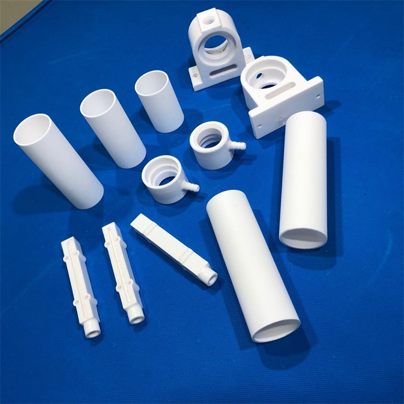
Yttrium oxide ceramic is a high-purity, non-oxide ceramic material produced from yttria powder through advanced sintering processes. It belongs to the rare earth oxide family and is characterized by its cubic crystal structure, which contributes to its exceptional chemical inertness and thermal stability. With a melting point of 2,430°C and density exceeding 4.98 g/cm³ for fully densified parts, yttrium oxide exhibits thermodynamic stability that few other ceramics can match .
In semiconductor manufacturing, yttrium oxide is typically fabricated as sintered bodies with purity levels of 99.9% or higher, often incorporating controlled additions of aluminum oxide (0.1–0.5 mass%) to optimize mechanical strength while maintaining plasma resistance . The material is available in various forms, including precision-machined components, coatings, and custom-manufactured parts tailored to specific equipment designs.
Key Properties of Yttrium Oxide Ceramics
Plasma Erosion Resistance
The most distinguishing characteristic of yttrium oxide is its superior resistance to halogen-based plasmas used in dry etching processes. Research has demonstrated that yttria exhibits significantly lower erosion rates compared to alumina in CF₄/CHF₃ plasma environments. While solid alumina erodes at approximately 1.44 μm/hr and pure yttria at 0.3 μm/hr, certain yttria-zirconia solid solutions can achieve rates as low as 0.1 μm/hr—a tenfold improvement over alumina . This resistance stems from the formation of stable yttrium fluorides that do not readily volatilize, unlike the aluminum fluorides that form and spall from alumina surfaces .
Corrosion Resistance
Yttrium oxide demonstrates outstanding resistance to corrosive gases and chemicals commonly encountered in semiconductor processing, including fluorine, chlorine, and other reactive species. The material’s thermodynamic stability ensures minimal reaction with process chemistries, significantly reducing particle generation and metal contamination risks .
Mechanical Properties
While yttrium oxide is not as mechanically robust as silicon carbide or zirconia, sintered bodies achieve respectable mechanical performance. Relative densities of 98% or higher are achievable through optimized processing, with fine grain structures contributing to enhanced strength . The material exhibits good flexural strength suitable for structural components, though design considerations should account for its moderate fracture toughness relative to alternative ceramics.
Electrical Insulation
Yttrium oxide offers excellent electrical insulation properties, with dielectric breakdown voltage comparable to alumina coatings. This characteristic makes it suitable for electrostatic chuck applications and other components requiring reliable electrical isolation in plasma environments . The material’s high purity is essential for maintaining consistent electrical performance and minimizing leakage currents.
High-Temperature Stability
With its exceptionally high melting point and thermal stability, yttrium oxide maintains structural integrity and chemical inertness across the full range of semiconductor processing temperatures. The material exhibits low thermal expansion and good thermal shock resistance, contributing to component reliability during thermal cycling.
Typical Applications in Semiconductor Equipment
Etch Chamber Components
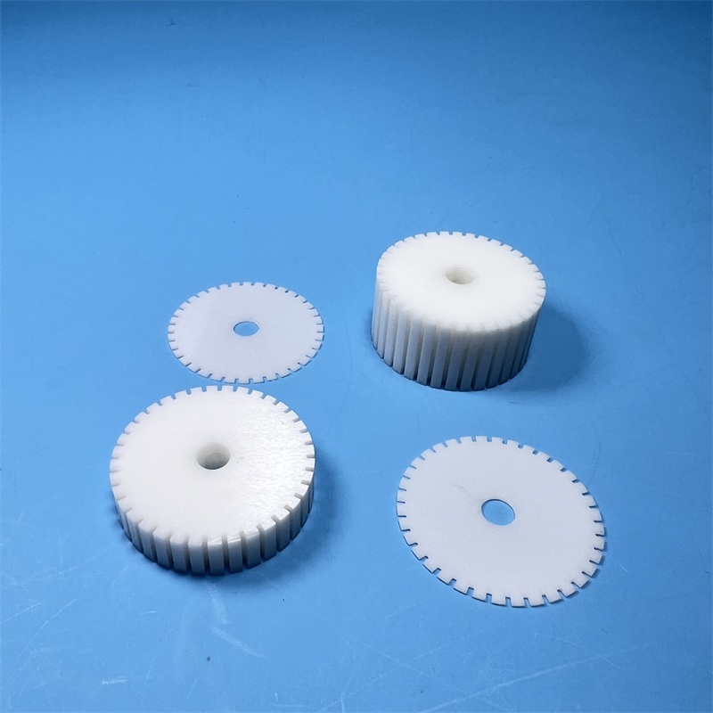
Yttrium oxide is most widely employed in plasma etch chambers, where components are directly exposed to highly reactive plasma environments. Key parts include:
– Focus rings that direct plasma density and maintain process uniformity
– Gas distribution plates that ensure uniform reactive gas flow across the wafer surface
– Protective liners and covers that shield chamber walls from plasma attack
– Showerhead electrodes requiring both plasma resistance and electrical functionality
Electrostatic Chucks
The material’s insulating properties, combined with its erosion resistance, make it suitable for electrostatic chuck components that must maintain precise wafer clamping while withstanding plasma exposure .
Process Chamber Liners
Full chamber liners fabricated from yttrium oxide provide extended service life compared to coated alternatives, reducing downtime for replacement and minimizing particle generation as the component ages .

Advantages Compared With Other Ceramic Materials
Yttrium Oxide vs. Alumina
Alumina (Al₂O₃) remains the most widely used ceramic in semiconductor equipment, but yttrium oxide offers compelling advantages in aggressive plasma environments. Where alumina forms volatile aluminum fluorides under fluorine-based plasma exposure—leading to surface degradation and particle contamination—yttria forms stable compounds that resist erosion . Additionally, the lower transition metal content in high-purity yttria reduces the risk of metallic contamination that can degrade device performance.
Yttrium Oxide vs. Yttria Coatings
While yttria can be applied as a plasma-sprayed coating, bulk yttria ceramics offer longer service life and superior performance. Solid yttria components eliminate coating adhesion concerns and the risk of coating delamination under process conditions. The dense, pore-free microstructure of sintered bodies provides more consistent erosion resistance than sprayed coatings .
Yttrium Oxide vs. Silicon Carbide
Silicon carbide (SiC) offers superior thermal conductivity and mechanical strength but is susceptible to chemical attack under certain plasma conditions. Yttrium oxide provides better chemical resistance in halogen-based environments, making it the preferred choice for parts directly exposed to reactive plasmas .
Custom Manufacturing Options
Precision Machining Capabilities
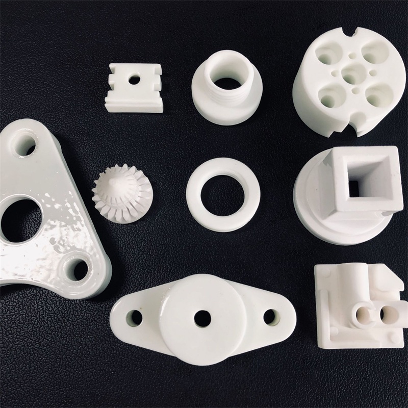
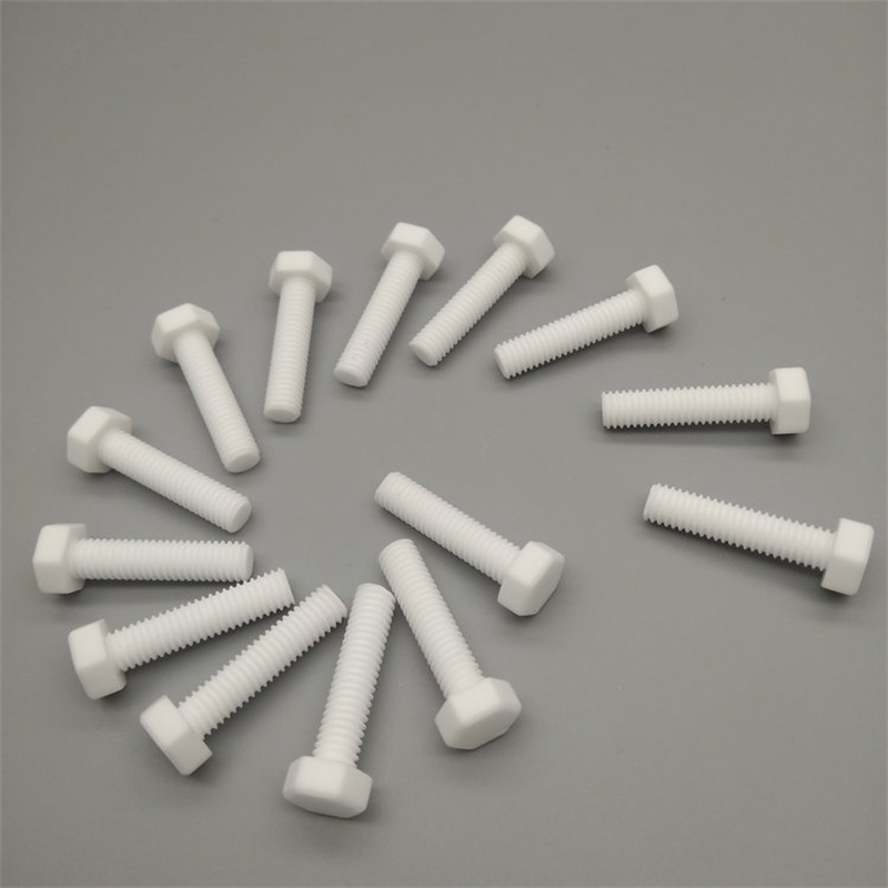
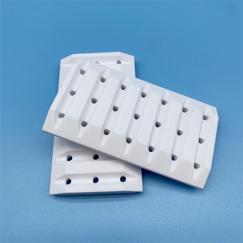
Established manufacturers with CNC machining centers and precision grinding equipment can produce yttrium oxide components to tight tolerances. Custom parts can be manufactured from both sintered blanks and near-net shapes, with dimensions tailored to specific equipment requirements .
Material Formulations
Custom components can be produced with controlled compositions, including yttria-zirconia solid solutions that offer enhanced plasma resistance and improved mechanical properties. Additives such as alumina in the 0.1–0.5% range are sometimes employed to optimize sintering behavior and strength .
Quality Control
Reliable suppliers implement comprehensive quality assurance programs, including dimensional inspection, visual examination, and functional testing of finished components. Raw material traceability and process documentation support the rigorous quality requirements of semiconductor applications .
How to Choose the Right Supplier
Evaluate Technical Capability
Qualified suppliers should demonstrate:
– Established experience with yttrium oxide processing and semiconductor applications
– In-house precision machining capabilities for complex geometries
– Documented quality systems (ISO 9001 or equivalent)
– Cleanroom manufacturing and packaging capabilities
Assess Purity and Process Control
Semiconductor applications demand high-purity materials. When evaluating potential suppliers, request:
– Certificates of Analysis (COA) confirming material composition and purity levels
– Information on raw material sourcing and traceability
– Process control documentation and statistical process control (SPC) data
Consider Total Cost of Ownership
While initial material costs for yttrium oxide exceed conventional ceramics, the extended component life and reduced contamination risks often result in lower total cost of ownership. Evaluate suppliers on long-term reliability rather than first cost alone.
Review Custom Manufacturing Experience
Select suppliers with demonstrated experience in producing complex Custom Parts and Precision Components for semiconductor applications. Experience with your specific equipment type and operating conditions is valuable.
Yttrium oxide ceramics have established themselves as the preferred material solution for critical components in semiconductor plasma etch equipment. The material’s exceptional resistance to plasma erosion, combined with its chemical stability and electrical insulation properties, enables longer component life, reduced particle generation, and improved process stability compared to traditional ceramic alternatives.
For procurement professionals and design engineers, successful application depends on appropriate component design, careful specification, and selection of a qualified Manufacturer or Supplier with proven capabilities in yttrium oxide processing. As semiconductor technology continues to advance toward smaller nodes and more aggressive process chemistries, the role of yttrium oxide ceramics in enabling manufacturing performance will continue to expand.
FAQ
What makes yttrium oxide better than alumina for semiconductor etch applications?
Yttrium oxide exhibits significantly superior resistance to halogen-based plasmas. Unlike alumina, which forms volatile aluminum fluorides that erode and generate particles, yttria forms stable compounds that resist etching. Independent studies show yttria ceramics can have erosion rates up to 10 times lower than alumina under identical plasma conditions .
What purity level is required for semiconductor-grade yttrium oxide components?
Semiconductor applications typically require purity of 99.9% or higher to minimize metal contamination risks. Manufacturers often incorporate controlled amounts of alumina (0.1–0.5%) to optimize mechanical properties while maintaining plasma resistance. Full densification with relative density exceeding 98% is essential for achieving optimal performance .
Can yttrium oxide be custom machined into complex geometries?
Yes, established suppliers with precision machining capabilities can produce Custom Parts with complex geometries from sintered yttria blanks. Near-net shape forming combined with CNC grinding and precision finishing enables production of intricate components such as gas distribution plates, focus rings, and chamber liners to tight tolerances .
What should I consider when selecting an yttrium oxide component supplier?
Key selection criteria include documented experience with semiconductor applications, purity verification through Certificates of Analysis, in-house precision machining capabilities, cleanroom manufacturing processes, and quality system certification. Requesting reference parts and reviewing quality documentation can help evaluate technical capability .
 What Is Polyimide (PI)
What Is Polyphenylene Sulfide (PPS)
What Is Polyimide (PI)
What Is Polyphenylene Sulfide (PPS)
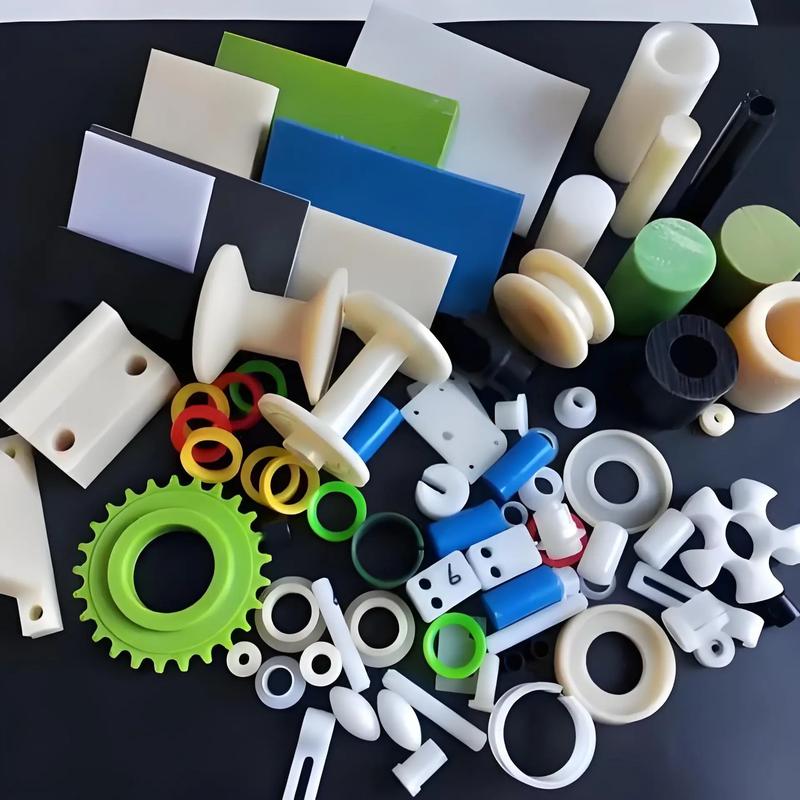 What is PEEK-for Engineers and Buyers
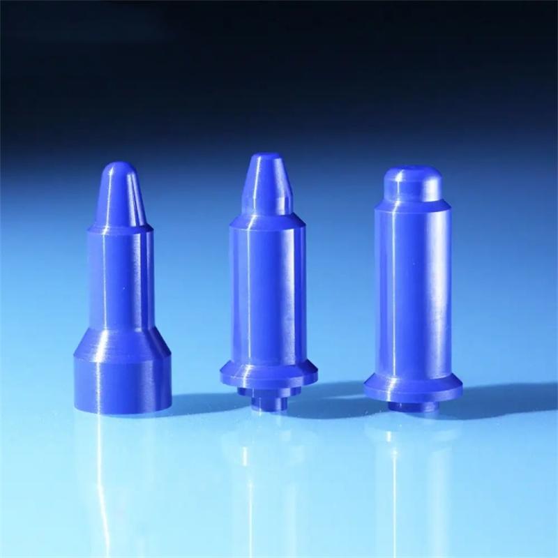 Application Scope of Zirconia Ceramic Structural Components