
Silicon Carbide Ceramics in Semiconductor Manufacturing Equipment
In the precision-driven world of semiconductor fabrication, equipment performance directly determines device yield and reliability. Silicon carbide (SiC) ceramics have emerged as an indispensable material for critical semiconductor manufacturing components, offering a unique combination of mechanical robustness, thermal stability, and chemical inertness that conventional materials cannot match.
Silicon carbide is a synthetic ceramic compound composed of silicon and carbon, characterized by strong covalent bonding that gives it exceptional hardness and high-temperature stability. Since its commercialization as an advanced ceramic in the early 1990s, SiC has become one of the most commercially significant technical ceramics globally, with semiconductor applications representing a major growth sector . As semiconductor device geometries continue to shrink and process temperatures rise, silicon carbide’s superior properties make it an increasingly vital material for equipment manufacturers and semiconductor fabs worldwide.
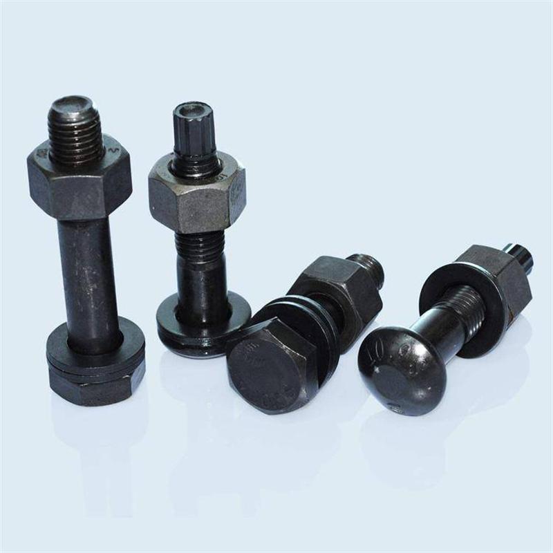
What Is Silicon Carbide Ceramic?
Silicon carbide (SiC) is a crystalline compound of silicon and carbon with a diamond-like tetrahedral structure. Over 150 known polytypes exist, though only a few are commonly found in commercial ceramics . The material exhibits approximately 88% covalent bonding, making it the fourth hardest known material and endowing it with exceptional mechanical and thermal properties.
For semiconductor equipment applications, SiC is typically manufactured through several processes: pressureless sintering (SSiC), reaction bonding (SiSiC), or hot pressing. Solid-phase sintered silicon carbide is particularly valued for semiconductor applications due to its ability to maintain strength even at temperatures up to 1400°C . The material’s inherent semiconductivity, combined with its high thermal conductivity, makes it uniquely suited for applications requiring both structural integrity and thermal management.
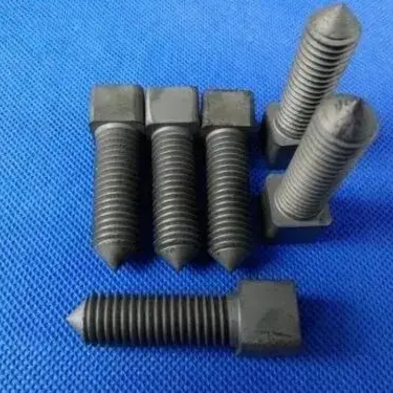
Key Properties Of Silicon Carbide Ceramics
Mechanical Properties
Silicon carbide exhibits outstanding mechanical characteristics essential for precision semiconductor equipment. Its flexural strength typically ranges from 400–450 MPa, with a modulus of elasticity between 207–483 GPa depending on processing methods . The material’s Vickers hardness of 2400–2800 HV provides exceptional wear resistance, ensuring dimensional stability during repeated wafer handling and processing . With a density of approximately 3.21 g/cm³, SiC is significantly lighter than alumina (4.0 g/cm³), offering an excellent strength-to-weight ratio .
Thermal Properties
Thermal management is critical in semiconductor processing. Silicon carbide delivers outstanding thermal conductivity of 120–180 W/m·K, enabling rapid heat dissipation from processing zones . Its coefficient of thermal expansion (CTE) of approximately 4.2×10⁻⁶/K closely matches that of silicon wafers, minimizing thermal stress and warpage during temperature cycling . This thermal expansion compatibility is particularly valuable for wafer carriers, vacuum chucks, and other components that maintain critical dimensional relationships with silicon wafers.
Chemical Resistance
Semiconductor manufacturing involves aggressive chemicals and plasma environments. Silicon carbide provides high resistance to plasma erosion and excellent acid resistance, including against hydrofluoric and hydrochloric acids . This chemical stability ensures minimal particle generation and contamination, crucial factors in maintaining cleanroom conditions and high device yields.
Electrical Properties
While generally considered semiconductive, sintered silicon carbide offers a range of electrical resistivity (10⁵–10⁶ Ω·cm) that can be tailored for specific applications . This tunable conductivity is valuable for electrostatic chucks and other components requiring controlled charge dissipation.
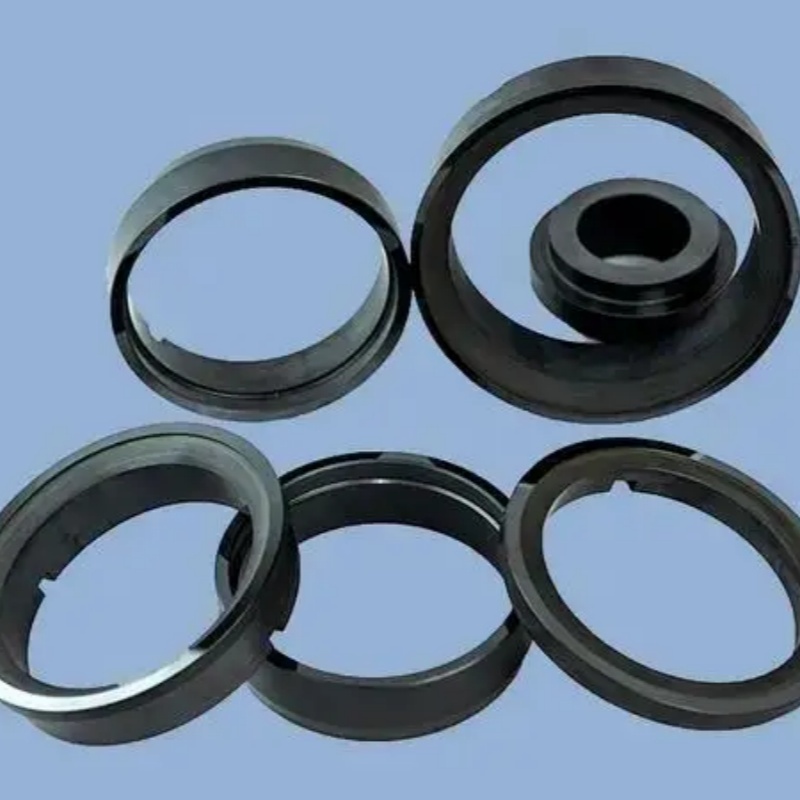
Typical Applications in Semiconductor Manufacturing
Wafer Handling and Processing
Silicon carbide components are extensively used in wafer handling equipment, including wafer carriers, transfer arms, and vacuum chucks. The material’s thermal expansion match to silicon and exceptional flatness make it ideal for low-mass wafer carrier components requiring dimensional stability during thermal processing .
Thermal Processing Equipment
In diffusion furnaces, oxidation tubes, and rapid thermal processing systems, silicon carbide provides the high-temperature resistance and chemical inertness essential for reliable operation. Components such as thermocouple protection tubes and furnace liners benefit from SiC’s ability to withstand extreme temperatures while maintaining structural integrity .
Etching and Deposition Chambers
Plasma etching and chemical vapor deposition (CVD) systems employ silicon carbide components that resist plasma erosion and maintain dimensional stability under aggressive conditions. The material’s high stiffness and low thermal expansion are particularly valuable in high-acceleration handling systems where dynamic micro-vibrations must be suppressed to reduce equipment settling time .
Metrology and Inspection
SiC’s dimensional stability and low thermal expansion make it suitable for air-bearing stages and positioning equipment used in semiconductor metrology . These applications demand exceptional flatness and rigidity for precise wafer inspection.

Advantages Compared With Other Ceramic Materials
vs. Alumina (Al₂O₃)
While alumina remains the most widely used ceramic in semiconductor equipment, silicon carbide offers superior thermal conductivity (120–180 W/m·K compared to 25–30 W/m·K) and a closer CTE match to silicon . SiC’s thermal expansion of approximately 4.2×10⁻⁶/K compares favorably to alumina’s 7.8×10⁻⁶/K, significantly reducing thermal stress in silicon-contacting components. However, alumina provides higher electrical resistivity (>10¹⁴ Ω·cm), making it preferable for applications requiring complete electrical isolation.
vs. Silicon Nitride (Si₃N₄)
Silicon nitride offers higher flexural strength (700–900 MPa vs. 400–450 MPa for SiC) and better fracture toughness, making it suitable for load-bearing components . However, SiC provides superior thermal conductivity and better plasma resistance, advantages that often outweigh the mechanical trade-offs in thermal management applications.
vs. Aluminum Nitride (AlN)
Aluminum nitride delivers the highest thermal conductivity (170–200 W/m·K) and excellent electrical insulation, making it ideal for heat-spreading applications requiring electrical isolation . However, SiC offers greater mechanical strength and wear resistance, with thermal conductivity that still substantially exceeds most engineering ceramics. The choice between these materials depends on whether thermal dissipation or mechanical robustness is the primary constraint.
vs. Quartz and Metals
Compared to quartz components, SiC offers far greater mechanical strength and thermal shock resistance. Unlike metals such as stainless steel or aluminum, SiC provides corrosion resistance, high-temperature stability, and a thermal expansion coefficient closely matched to silicon, eliminating contamination risks and thermal mismatch issues.
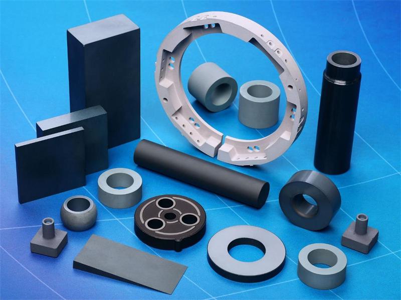
Custom Manufacturing Options
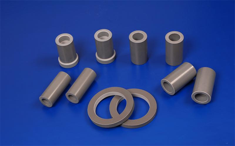
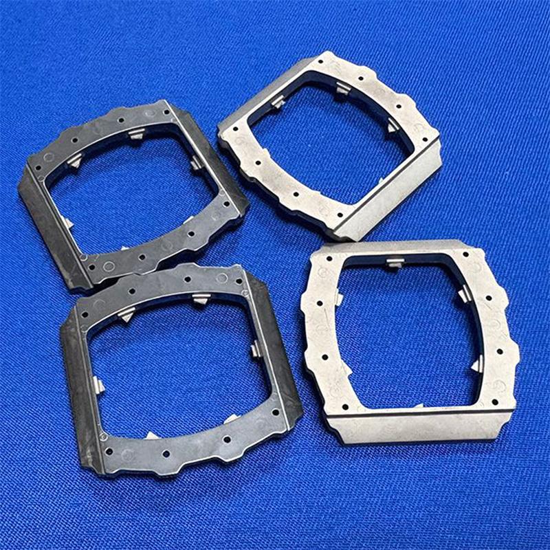
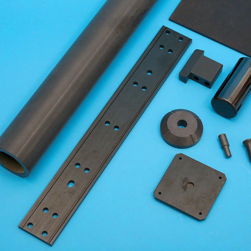
Precision machining services for silicon carbide components typically encompass several manufacturing approaches. Custom Parts can be produced through pressing and sintering, followed by precision grinding and lapping. OEM ceramic components are manufactured to exact specifications using CNC machining capabilities that can achieve extremely tight tolerances .
Several custom manufacturing techniques are available:
Green Machining involves machining components before sintering when the material is in a softer, more workable state. This approach is cost-effective for complex geometries and can be followed by full densification.
Hard Machining uses diamond grinding tools on fully densified material to achieve final dimensions. This technique is essential for precision components requiring tight tolerances and excellent surface finishes.
Injection Molding enables high-volume production of complex shapes with consistent quality, suitable for components with intricate internal features.
Lapping and Polishing achieves the ultra-smooth surfaces (Ra ≤ 5–10 nm) required for wafer-contacting components and sealing surfaces .
Capabilities include micro-hole drilling (diameters as small as 0.02 mm), achieving stringent flatness requirements, and optical-grade mirror surface polishing .
How To Choose The Right Supplier
Selecting a reliable Manufacturer or Supplier of silicon carbide Precision Components requires careful evaluation of several factors.
Technical Capabilities
Evaluate the supplier’s experience with silicon carbide processing. Does the company have demonstrated expertise in both material processing and precision machining? A credible supplier should offer comprehensive technical data sheets documenting material properties, including Mechanical Properties, thermal conductivity, and other key performance metrics. The ability to provide custom-tailored solutions rather than only catalog items distinguishes high-quality suppliers.
Quality Systems and Certifications
Reputable manufacturers maintain ISO 9001 and AS9100 certifications . Look for companies with established quality management systems that include statistical process control, material traceability, and dimensional inspection documentation.
Industry Experience
Preference should be given to suppliers with proven track records in the semiconductor industry. Experience with semiconductor-specific applications demonstrates understanding of cleanliness requirements, particle control, and the importance of minimizing contamination risks.
Manufacturing Flexibility
Assess the supplier’s ability to handle everything from prototypes to full production runs. Companies offering comprehensive services from material processing through final finishing typically provide better quality control and shorter lead times.
Supply Chain Reliability
Evaluate the Factory’s capacity, typical lead times, and ability to meet delivery schedules. For critical components, redundancy in manufacturing capabilities and transparent communication regarding production status are essential.
Silicon carbide ceramics occupy a critical position in semiconductor manufacturing equipment, offering a combination of mechanical, thermal, and chemical properties unmatched by alternative materials. From wafer carriers and vacuum chucks to plasma etching components and metrology stages, SiC enables the precision, reliability, and contamination control essential for modern semiconductor fabrication.
When selecting silicon carbide components, careful attention to material specifications, manufacturing processes, and supplier capabilities ensures that the final components meet the demanding requirements of semiconductor applications. The material’s exceptional thermal conductivity, wear resistance, and thermal expansion compatibility with silicon make it an increasingly important choice as semiconductor process complexity and performance requirements continue to escalate.
As the semiconductor industry advances toward smaller geometries and more demanding processes, silicon carbide’s proven performance positions it as a foundational material for next-generation equipment.
Frequently Asked Questions(FAQ)
What is the difference between silicon carbide and alumina ceramics for semiconductor applications?
Silicon carbide offers superior thermal conductivity (120–180 W/m·K vs. 25–30 W/m·K for alumina) and a coefficient of thermal expansion (4.2×10⁻⁶/K) much closer to silicon than alumina (7.8×10⁻⁶/K). This reduces thermal stress in wafer-contacting components. However, alumina provides higher electrical resistivity, making it preferable when complete electrical isolation is required. Alumina is also more cost-effective for less demanding applications.
What temperature can silicon carbide withstand in semiconductor processing equipment?
Solid-phase sintered silicon carbide maintains its mechanical strength even at temperatures up to 1400°C . The maximum continuous service temperature is approximately 1600°C in inert atmospheres, though oxidation resistance allows reliable service at high temperatures in air as well .
Why is silicon carbide used in electrostatic chucks and wafer carriers?
Silicon carbide’s thermal expansion coefficient closely matches that of silicon, minimizing thermal stress-induced wafer warping during temperature cycling. Its high elastic modulus (approximately twice that of alumina) provides excellent dimensional stability, suppressing dynamic vibrations that can affect processing precision. The material’s high thermal conductivity enables rapid thermal equilibration, eliminating localized hot spots and maintaining wafer flatness .
How do I choose a silicon carbide component supplier for semiconductor equipment?
Evaluate suppliers based on: (1) demonstrated experience with precision-machined silicon carbide components, (2) quality certifications such as ISO 9001 or AS9100, (3) technical capabilities including material processing and machining services, (4) industry references and track record in semiconductor applications, and (5) manufacturing flexibility for both prototyping and production volumes .
Is silicon carbide ceramic suitable for plasma etching environments?
Yes, silicon carbide offers high plasma resistance and excellent acid resistance, including against hydrofluoric and hydrochloric acids. This chemical stability ensures minimal particle generation and contamination in plasma etching environments. The material’s exceptional corrosion resistance makes it a preferred choice for components exposed to aggressive plasma chemistries .
 What Is Polyimide (PI)
What Is Polyphenylene Sulfide (PPS)
What Is Polyimide (PI)
What Is Polyphenylene Sulfide (PPS)
 What is PEEK-for Engineers and Buyers
 Application Scope of Zirconia Ceramic Structural Components