
Semiconductor Manufacturing Specialty Materials
The semiconductor industry operates at the forefront of materials science, where the choice of materials directly determines device performance, manufacturing yield, and long-term reliability. As chip architectures become increasingly complex and fabrication processes push toward atomic-scale precision, understanding the distinct roles of metals, ceramics, and polymers has become essential for engineers, procurement specialists, and product designers involved in semiconductor manufacturing and packaging.
Semiconductor manufacturing relies on three broad categories of specialty materials, each serving fundamentally different functions. Metals dominate electrical interconnections and heat dissipation. Advanced ceramics provide the thermal stability, chemical resistance, and electrical insulation required in extreme fabrication environments. Polymers offer cost-effective encapsulation and dielectric layers for device protection . The optimal selection among these material families requires careful evaluation of thermal, mechanical, electrical, and chemical properties, as well as the specific performance requirements of each application.
What Are Semiconductor Specialty Materials?
Semiconductor specialty materials are engineered substances specifically designed to meet the stringent requirements of semiconductor device fabrication, packaging, and thermal management. Unlike conventional industrial materials, these specialized materials must exhibit extremely high purity, precise compositional control, and predictable performance under demanding conditions that include high temperatures, corrosive chemical environments, plasma exposure, and rapid thermal cycling.
These materials serve diverse functions throughout the semiconductor manufacturing ecosystem. In device fabrication, they form the structural layers, conductive pathways, and dielectric insulators that constitute integrated circuits. In packaging, they protect delicate chips from environmental damage while managing electrical connections and dissipating heat. In manufacturing equipment, they provide wear-resistant, chemically stable components that maintain process integrity over extended production runs.
Material Categories: Composition and Structure
Metals in Semiconductor Manufacturing
Metals serve primarily as conductors in semiconductor applications, valued for their exceptional electrical and thermal conductivity. The selection of specific metals depends on the performance requirements of each application, including conductivity, thermal management, resistance to oxidation and corrosion, and cost considerations .
Copper dominates interconnection applications due to its excellent electrical conductivity, which is second only to silver. Its relatively low cost and established processing infrastructure make it the standard choice for on-chip interconnects and metallization layers. However, copper’s lower melting point compared to refractory metals limits its use in high-temperature processes .
Tungsten offers exceptional high-temperature stability with a melting point of 3422°C, making it the preferred material for barrier layers and diffusion layers where thermal stability is critical. Its body-centered cubic crystal structure provides superior mechanical strength and thermal stability under high-energy ion bombardment. While tungsten exhibits lower conductivity than copper, its chemical stability and oxidation resistance in aggressive environments compensate for this limitation .
Aluminum, despite being gradually replaced by copper in many interconnect applications, remains relevant for certain packaging and heat sink applications due to its low density, good thermal conductivity, and cost-effectiveness . Gold finds application in high-reliability packaging where its oxidation resistance and consistent electrical performance justify the higher cost.
Advanced Ceramics in Semiconductor Manufacturing
Advanced ceramics, also known as engineered or technical ceramics, constitute the most diverse material category in semiconductor applications. These materials are designed through precise compositional control and manufacturing processes to achieve specific electrical, thermal, and mechanical properties essential for semiconductor processing .
The defining characteristic of advanced ceramics is their combination of high-temperature stability, excellent electrical insulation, chemical inertness, and mechanical durability. Unlike traditional ceramics used in construction or pottery, semiconductor-grade ceramics are engineered with controlled microstructure and precisely defined properties .
Aluminum oxide (Al₂O₃) represents the most widely used advanced ceramic, comprising approximately 90% of ceramic substrate applications . Its popularity stems from the optimal balance of electrical insulation, thermal conductivity, mechanical strength, and economic viability. The material exhibits volume resistivity high enough for electrical insulation requirements and thermal conductivity of approximately 20-30 W/(m·K), sufficient for many substrate applications .
Silicon carbide (SiC) offers superior thermal conductivity of 120-200 W/(m·K), approximately 6-8 times that of aluminum oxide, combined with exceptional hardness (Mohs hardness 9.5) and chemical stability. Its high thermal conductivity and mechanical strength make it ideal for applications requiring rapid heat dissipation and structural integrity under thermal stress. SiC components can maintain structural integrity up to 1600°C in inert atmospheres .
Aluminum nitride (AlN) is emerging as a critically important ceramic for high-performance semiconductor packaging. It combines thermal conductivity approaching that of silicon carbide (approximately 170 W/(m·K)) with a thermal expansion coefficient well-matched to silicon. Its low density enables weight reductions of approximately 20% compared to aluminum oxide components, and its fracture strength exceeds that of aluminum oxide. The material’s dielectric properties and chemical stability make it a leading candidate for next-generation high-density packaging and substrate applications .
Silicon nitride (Si₃N₄) offers exceptional fracture toughness and thermal shock resistance, making it valuable for components subject to mechanical stress. Its electrical insulation properties and high-temperature stability complement its mechanical performance.
Zirconia (ZrO₂) provides the highest fracture toughness among advanced ceramics, along with excellent thermal shock resistance. These properties make it suitable for wafer handling components and processing tools that must withstand thermal cycling .
Polymers in Semiconductor Manufacturing
Polymers serve critical functions in semiconductor packaging and device protection, valued for their light weight, low cost, electrical insulation properties, and ease of processing. However, the intrinsic thermal limitations of polymers restrict their use to applications where extreme temperatures are not encountered .
Epoxy resins represent the dominant polymer class in semiconductor packaging. These thermosetting polymers offer an advantageous combination of electrical insulation properties, chemical resistance, thermal stability, and processing flexibility. Epoxies can be formulated with various fillers to enhance thermal conductivity or reduce cost, and they form protective encapsulation that shields chips from environmental contaminants .
Polyimides provide superior thermal stability and mechanical strength compared to epoxy resins, making them suitable for high-temperature packaging applications. Their excellent adhesion properties enable reliable bonding with metals and ceramics, and their resistance to harsh processing chemicals extends component lifetime .
Acrylic resins find application primarily in optoelectronic device packaging where their transparency and chemical stability are advantageous. These polymers can be rapidly cured using ultraviolet light, increasing manufacturing throughput .
Key Properties Comparison
Thermal Properties
Thermal management is paramount in semiconductor manufacturing, where power densities continue to increase and temperature control directly affects process yield and device reliability. The three material categories exhibit fundamentally different thermal behaviors.
Metals provide the highest thermal conductivity among the three material categories, with copper achieving approximately 401 W/(m·K) and aluminum approximately 237 W/(m·K). Tungsten, while lower in conductivity at 173 W/(m·K), maintains its thermal performance at elevated temperatures where other metals would degrade. However, the coefficient of thermal expansion of metals is substantially higher than that of silicon, creating stress challenges at material interfaces.
Advanced ceramics offer a broader range of thermal properties. Silicon carbide and aluminum nitride both achieve thermal conductivity values exceeding 100 W/(m·K), approaching those of metals while providing electrical insulation that metals cannot offer. Aluminum oxide provides moderate thermal conductivity of 20-30 W/(m·K), which, while lower, remains sufficient for many applications . More critically, ceramic thermal expansion coefficients can be engineered to match silicon, reducing interfacial stress and improving device reliability .
Polymers have thermal conductivity values typically below 1 W/(m·K), orders of magnitude lower than either metals or ceramics. This limitation prevents polymer use in applications requiring efficient heat dissipation. Their service temperatures are also substantially lower, typically below 200°C for most formulations .
Electrical Properties
Electrical conductivity and insulation requirements vary widely across semiconductor applications. Metals provide the highest electrical conductivity, with copper and aluminum enabling efficient current conduction in interconnects and packaging.
Ceramics generally provide excellent electrical insulation, with aluminum oxide and aluminum nitride offering high volume resistivity and dielectric strength. This combination of thermal conductivity and electrical insulation makes ceramics uniquely valuable for applications such as electrostatic chucks, where electrical isolation must coexist with heat transfer. An exception is conventional silicon carbide, which exhibits semiconductor behavior and can be conductive unless specifically processed to achieve high resistivity .
Polymers offer good electrical insulation properties comparable to ceramics, with high dielectric strength and low dielectric constants. For high-frequency applications, polymer dielectrics can reduce signal propagation delays compared to ceramics, making them valuable for certain packaging configurations .
Mechanical Properties
The mechanical requirements of semiconductor materials vary by application. Components such as wafer handling robots, processing chambers, and sealing components must withstand wear, mechanical stress, and thermal cycling.
Metals generally offer high ductility and fracture toughness, reducing the risk of catastrophic failure. This mechanical robustness makes them reliable for structural applications, though their thermal expansion mismatch with silicon must be carefully managed.
Advanced ceramics exhibit high hardness and compressive strength but are brittle, requiring careful design to prevent fracture. Silicon carbide’s Mohs hardness of 9.5 (second only to diamond) makes it exceptionally wear-resistant, while aluminum oxide at 9.0 provides substantial wear resistance . Zirconia offers a higher fracture toughness than most ceramics, reducing brittleness concerns . Carbon materials such as diamond exhibit extreme hardness and thermal conductivity exceeding 2200 W/(m·K) at room temperature, approximately 13 times that of silicon .
Polymers provide excellent fracture resistance and mechanical flexibility but lack the high-temperature strength and rigidity of ceramics and metals.
Chemical Properties
Semiconductor manufacturing exposes materials to aggressive chemicals including acids, bases, solvents, and reactive plasmas. Chemical stability directly affects component lifetime and process contamination.
Metals vary widely in their chemical resistance. Noble metals such as gold resist oxidation and corrosion, while copper and aluminum are susceptible to oxidation and require protective barriers in many environments.
Advanced ceramics generally provide excellent chemical stability, with silicon carbide particularly resistant to halogen plasmas used in etching processes . Aluminum nitride and aluminum oxide exhibit good chemical resistance in most semiconductor processing environments.
Polymers offer resistance to many chemicals but are susceptible to degradation at elevated temperatures or under plasma exposure, requiring careful selection for specific process conditions.
Manufacturing and Processing Considerations
Metal Processing
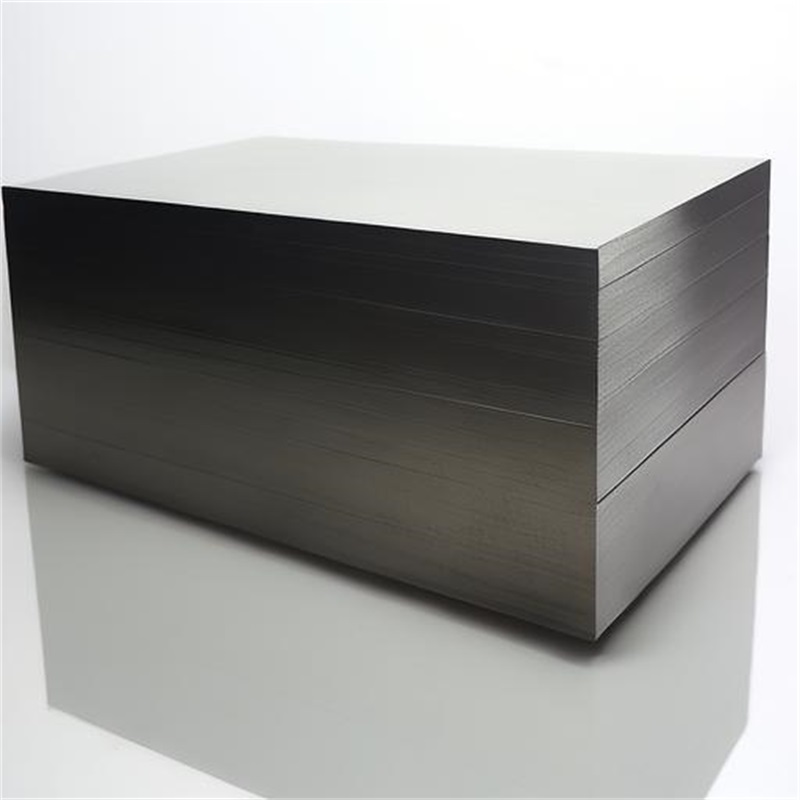
Metal components in semiconductor manufacturing are typically fabricated through conventional metallurgical processes including casting, forging, rolling, and machining. Thin-film deposition for interconnects and metallization layers employs physical vapor deposition (PVD) processes such as sputtering, as well as chemical vapor deposition (CVD) and electroplating for specific applications.
For sputtering targets, purity requirements are extremely stringent. Copper and aluminum targets are manufactured with high purity levels to prevent film contamination. Tungsten targets, while more expensive and difficult to machine, offer superior high-temperature stability and produce denser, more uniform films compared to alternative materials .
Ceramic Processing
The processing of advanced ceramics for semiconductor applications requires careful control of raw material purity, forming methods, and sintering conditions to achieve the required density, microstructure, and properties. Key processing steps include powder synthesis, forming (uniaxial pressing, isostatic pressing, or casting), sintering at elevated temperatures, and machining to final dimensions.
Aluminum oxide components are typically sintered at approximately 1500-1600°C, while silicon carbide requires sintering temperatures above 2000°C, contributing to its higher cost . The complexity of silicon carbide processing, including the difficulty of achieving high-density parts without defects, results in component costs approximately 2-5 times higher than aluminum oxide equivalents.
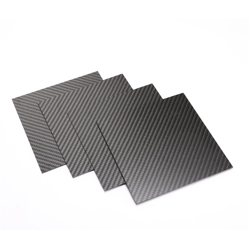
For silicon carbide substrates, fabrication approaches such as liquid silicon infiltration (LSI) of carbon fiber preforms have been developed to produce large-scale components while managing the inherent brittleness of single-phase ceramics .
Polymer Processing
Polymers in semiconductor packaging are processed through established techniques including injection molding, transfer molding, and casting. Epoxy molding compounds are the predominant encapsulation materials, processed through transfer molding at moderate temperatures and pressures. The ability to cure at temperatures compatible with device thermal budgets is a significant advantage of polymer systems.
Applications Across the Semiconductor Industry
Device Fabrication Applications
In the fabrication of semiconductor devices, materials play critical roles at every process step. The selection among metals, ceramics, and polymers depends on specific functional requirements at each stage.
Metals in Device Fabrication
Copper and aluminum are used to form the conductive interconnects that connect individual transistors and devices into working circuits. Copper has become the dominant interconnect material due to its high conductivity and resistance to electromigration, though its susceptibility to diffusion through dielectric layers requires barrier layers of materials such as tantalum, titanium, or tungsten.
Tungsten is essential for forming contact plugs and barrier layers, particularly where high-temperature stability is required. Its high melting point allows it to withstand subsequent process steps without degradation . Molybdenum is increasingly used in advanced deposition processes such as atomic layer deposition (ALD) for its properties in forming conformal films in complex 3D device architectures .
Ceramics in Device Fabrication
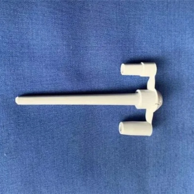
Advanced ceramics serve critical functions in the fabrication environment itself. Process chambers, wafer handling components, and tooling are fabricated from ceramics to ensure low contamination, chemical stability, and wear resistance. Key applications include:
Ceramic wafer handling components such as vacuum chucks and wafer carriers, where the combination of mechanical durability and chemical stability is essential . Electrostatic chucks (E-chucks) require the careful selection of ceramic materials for the dielectric layer to provide electrical insulation while allowing efficient heat transfer. In these applications, aluminum oxide often serves as the dielectric layer while silicon carbide provides the high thermal conductivity needed for heat dissipation .
Ceramic components in etch chambers and deposition tools are exposed to aggressive plasmas and require high chemical resistance. Silicon carbide’s resistance to halogen plasmas makes it a preferred material for etch chamber components . Ceramic mechanical components such as robot arms benefit from the high specific stiffness of silicon carbide, enabling precise positioning with minimal deflection in long-reach configurations.
Device Packaging Applications
Semiconductor packaging protects chips from environmental stress while providing electrical connections and thermal management. The choice between metal, ceramic, and polymer packaging significantly affects device reliability, performance, and cost.
Ceramic Packaging
Ceramic packaging offers the highest reliability among packaging types, with exceptional thermal stability, hermetic sealing, and performance under extreme conditions. This makes ceramic packaging the standard for aerospace applications, military systems, and high-reliability industrial electronics that require exceptional performance and long-term durability .
Aluminum oxide-based packaging, while offering moderate thermal conductivity (approximately 20-30 W/(m·K)), provides the optimal combination of electrical insulation, mechanical strength, and cost for many applications . For higher-power devices, aluminum nitride packaging with its superior thermal conductivity of approximately 170 W/(m·K) is increasingly specified, though the higher cost remains a limiting factor for broader adoption .
Polymer Packaging
Polymer packaging represents the most widely used packaging type, particularly for consumer electronics and commercial applications where cost is paramount. Epoxy molding compounds provide adequate protection for many device types at significantly lower cost than ceramic alternatives. However, the lower thermal conductivity and reliability compared to ceramics restrict their use in demanding applications .
Metal Packaging
Metal packaging provides excellent thermal conductivity and mechanical protection but faces challenges with thermal expansion mismatch with silicon, potentially leading to stress-related failures. The higher cost of metal packaging also limits its application to specific high-performance scenarios .
Thermal Management Applications
Power dissipation in semiconductor devices has become a critical challenge, particularly for artificial intelligence processors, high-performance computing, and power electronics. Heat generation continues to increase with device density and performance demands, requiring advanced thermal management solutions.
Diamond and Diamond Composites
Single-crystal diamond exhibits exceptional thermal conductivity of approximately 2200 W/(m·K) at room temperature, which is 13 times that of silicon. This property makes diamond heat spreaders and thermal management components increasingly vital for AI and high-performance computing applications. The global market for AI chip diamond heat spreaders is projected to reach approximately 59 billion RMB by 2030, reflecting a compound annual growth rate exceeding 50% .
Despite these advantages, diamond-based thermal management components face significant challenges. Production costs remain high, processing difficulties limit availability, and scaling to larger wafer sizes presents ongoing technical obstacles. The manufacturing cycle for diamond components is substantially longer than for conventional materials, and equipment costs are considerably higher .
Advanced Ceramic Substrates
Ceramic substrates play a central role in thermal management for power devices. Silicon nitride (Si₃N₄) substrates offer the highest fracture toughness among ceramics while providing adequate thermal conductivity for many applications. Aluminum nitride substrates combine high thermal conductivity with excellent thermal expansion matching to silicon, making them ideal for high-power applications where reliability is essential .
Advanced Deposition Technologies
Atomic layer deposition (ALD) and atomic layer etching (ALE) represent the forefront of semiconductor processing, enabling layer-by-layer atomic-scale fabrication. These processes require specialized precursor chemistries and materials that demonstrate unprecedented purity and reactivity.
For ALD, advanced precursors are being developed across the periodic table, including hafnium and zirconium compounds for high-k dielectrics, molybdenum and tungsten compounds for metal layers, and novel materials such as europium, lanthanum, and scandium for specialized applications. These precursors must achieve high film quality, excellent step coverage, and minimal impurities while maintaining stability during processing .
In ALE, careful materials selection enables precise etching of high-k materials such as hafnium oxide, zirconium oxide, and hafnium zirconium oxide. These processes are essential for integrating advanced transistors and memory stacks as device geometries continue to shrink .
Selection Guide for Engineers and Procurement
The selection of materials for semiconductor applications requires careful evaluation of multiple interdependent factors. Engineers and procurement professionals should follow a systematic approach to ensure optimal outcomes.
Application-Specific Selection Criteria
For each application category, specific material attributes take priority:
Substrate Applications (Heat Dissipation and Electrical Isolation)
When selecting substrate materials, thermal conductivity and electrical insulation are paramount. Aluminum oxide provides an economical baseline with thermal conductivity of 20-30 W/(m·K) and excellent electrical insulation. For higher thermal conductivity requirements, aluminum nitride (approximately 170 W/(m·K)) or silicon carbide (120-200 W/(m·K)) should be considered, with attention to the latter’s potential conductivity issues that may require specialty high-resistivity grades .
Packaging Applications (Protection and Interconnection)
For packaging decisions, reliability requirements, thermal budget, and cost drive the selection. Ceramic packaging offers superior hermetic sealing and high-temperature stability but at higher cost. Polymer packaging offers cost advantages but with lower thermal conductivity and reliability. Metal packaging provides excellent thermal performance but requires careful thermal expansion management .
Process Equipment Components (Wear and Corrosion Resistance)
Equipment components are selected based on exposure to process environments. Silicon carbide offers superior resistance to halogen plasma environments and is preferred for etch chambers and similar aggressive conditions. Aluminum oxide provides good chemical resistance and wear resistance at lower cost, making it suitable for less demanding applications. Zirconia offers outstanding fracture toughness and thermal shock resistance for components subject to mechanical stress .
Interconnect and Barrier Layer Applications
For on-chip interconnects, copper offers the highest conductivity but requires barrier layers to prevent diffusion. Tungsten provides superior high-temperature stability and chemical resistance for barrier and contact applications, though with lower electrical conductivity. Aluminum may be selected for applications where cost and weight are primary considerations, though its use in advanced nodes has been largely displaced by copper .
Cost Considerations
Cost remains a significant factor in materials selection. Aluminum oxide components are generally the most economically viable, with abundant raw materials and established processing infrastructure. Silicon carbide components typically cost 2-5 times more than aluminum oxide equivalents due to higher sintering temperatures (above 2000°C versus 1500-1600°C for alumina) and increased processing complexity .
Aluminum nitride, while offering superior thermal properties, commands a premium due to more complex processing and higher raw material costs. Diamond components are significantly more expensive due to limited manufacturing capacity and complex processing requirements .
Common Selection Pitfalls
Several common mistakes should be avoided when selecting semiconductor materials:
1. Overlooking thermal expansion mismatch: Selecting materials with thermal expansion coefficients significantly different from silicon can lead to stress-related failures during thermal cycling.
2. Underestimating contamination risks: Insufficient purity specifications for materials can introduce contamination that affects device yield and reliability.
3. Neglecting chemical compatibility: Materials that show adequate performance in one process environment may degrade in a different chemical environment, particularly when aggressive etch processes are involved.
4. Overlooking processing constraints: Materials with excellent final properties may require processing conditions incompatible with device thermal budgets or existing manufacturing infrastructure.
5. Focusing solely on initial cost: Materials selection should consider total cost of ownership, including yield effects, component lifetime, and maintenance requirements, rather than initial purchase price alone.
Industry Standards
Semiconductor materials are subject to rigorous industry standards that ensure consistency, purity, and reliability. These standards provide a foundation for specification and quality assurance throughout the supply chain.
Key standards relevant to semiconductor materials include:
SEMI International Standards establish material purity requirements, test methods, and specifications for semiconductor-grade materials. These standards are maintained by SEMI, the global industry association for the semiconductor and electronics manufacturing supply chain.
ASTM International provides test methods and specifications for materials characterization across the semiconductor industry, including standards for thermal conductivity measurement, mechanical properties testing, and chemical analysis.
ISO standards provide broader international specifications for material quality and testing procedures, complementing the more industry-specific standards.
Procurement professionals should verify that materials meet all relevant specifications and have been tested according to applicable standards. Documentation of conformance should be obtained from suppliers, and incoming materials inspection should include verification of critical purity and property parameters.
Frequently Asked Questions
What are the most commonly used metals in semiconductor manufacturing and why?
Copper is the primary metal for on-chip interconnects due to its high electrical conductivity and electromigration resistance. Tungsten is widely used for barrier layers and contact plugs where high-temperature stability is critical. Aluminum is used in some packaging and heat sink applications .
What advantages do advanced ceramics offer over metals in semiconductor manufacturing?
Advanced ceramics provide electrical insulation where metals cannot, enabling functions such as electrostatic chucks that combine electrical isolation with heat transfer. Ceramics also provide superior chemical resistance to corrosive process environments and better thermal expansion matching to silicon .
Why is aluminum nitride considered a promising material for semiconductor packaging?
Aluminum nitride combines high thermal conductivity of approximately 170 W/(m·K) with excellent electrical insulation, a thermal expansion coefficient well-matched to silicon, and low density that enables weight reduction. These properties make it ideal for high-power, high-reliability packaging applications .
What are the trade-offs between silicon carbide and aluminum oxide ceramics in semiconductor applications?
Silicon carbide offers significantly higher thermal conductivity (120-200 W/(m·K) versus 20-30 W/(m·K) for aluminum oxide) and superior resistance to plasma etching. However, aluminum oxide components typically cost 2-5 times less and provide excellent electrical insulation for most applications .
How do polymers compare to ceramics in semiconductor packaging?
Polymers offer lower cost, lighter weight, and easier processing compared to ceramics, making them attractive for consumer electronics. However, polymers have lower thermal conductivity and cannot match the hermetic sealing or high-temperature stability of ceramic packaging, limiting their use in high-reliability applications .
What is the role of diamond in semiconductor thermal management?
Diamond offers exceptional thermal conductivity of approximately 2200 W/(m·K), 13 times that of silicon. Diamond heat spreaders and thermal management components are becoming increasingly important for AI processors and high-performance computing applications where heat dissipation is a critical challenge .
What processing challenges are associated with ceramic materials?
Ceramic processing requires careful control of raw materials, forming processes, and high-temperature sintering. Silicon carbide requires sintering above 2000°C, contributing to higher costs. The inherent brittleness of ceramics also presents machining challenges, and defects during processing can lead to component failure .
Why is tungsten used as a sputtering target in semiconductor manufacturing?
Tungsten offers exceptional high-temperature stability with a melting point of 3422°C, superior mechanical strength, and excellent chemical stability in aggressive process environments. While tungsten has lower electrical conductivity than copper, its durability and thermal stability make it preferable for demanding sputtering applications .
The selection of specialty materials for semiconductor manufacturing demands a comprehensive understanding of the distinct performance characteristics of metals, advanced ceramics, and polymers. Each material category serves critical, complementary functions in the complex ecosystem of semiconductor device fabrication, packaging, and thermal management.
Metals provide essential electrical conductivity for interconnections and thermal management, with copper dominating interconnect applications due to its high conductivity, and refractory metals such as tungsten enabling high-temperature stability in barrier and contact applications. Advanced ceramics fill the unique role of providing electrical insulation while maintaining thermal conductivity, chemical resistance, and high-temperature stability, with aluminum oxide offering the best balance of cost and performance, aluminum nitride providing superior thermal properties for demanding applications, and silicon carbide delivering exceptional thermal conductivity and plasma resistance. Polymers offer cost-effective encapsulation solutions with adequate performance for commercial applications.
The selection among these materials depends on specific application requirements, including thermal conductivity, electrical insulation, chemical resistance, mechanical strength, and cost. Engineers and decision-makers must consider the complete system requirements, including thermal expansion matching, contamination control, processing compatibility, and total cost of ownership.
As semiconductor devices continue to advance toward atomic-scale precision and increasing power densities, the demands on specialty materials will intensify. Innovations in precursor chemistry for atomic layer deposition and etching, advancements in thermal management materials including diamond and ceramic composites, and continued refinement of packaging materials will enable next-generation device architectures. Understanding the fundamental properties and appropriate applications of metals, ceramics, and polymers remains essential for professionals across the semiconductor industry value chain.
Metals vs. Ceramics vs. Composites: Engineer’s Guide to Material Selection
Material Selection Guide for Corrosive Environments
Alloys vs. Ceramics vs. Polymers for High-Temperature Applications
Comparative Analysis of Automotive Lightweighting Materials