
Sapphire Ceramic in Semiconductor Manufacturing Equipment
Sapphire ceramic, a single-crystal form of aluminum oxide (Al₂O₃), has emerged as a critical material in semiconductor manufacturing equipment. Unlike polycrystalline alumina, sapphire is grown as a single crystal, eliminating grain boundaries and yielding exceptional mechanical, thermal, and chemical properties. Its unique combination of high-temperature stability, plasma resistance, and optical transparency makes it indispensable for demanding semiconductor fabrication processes, including etching, deposition, and lithography.
This guide provides a technical overview of sapphire ceramic for semiconductor applications, covering properties, specifications, comparative advantages, and procurement considerations. Whether you are a design engineer evaluating materials or a procurement specialist seeking a reliable manufacturer, this resource offers objective, data-driven guidance.
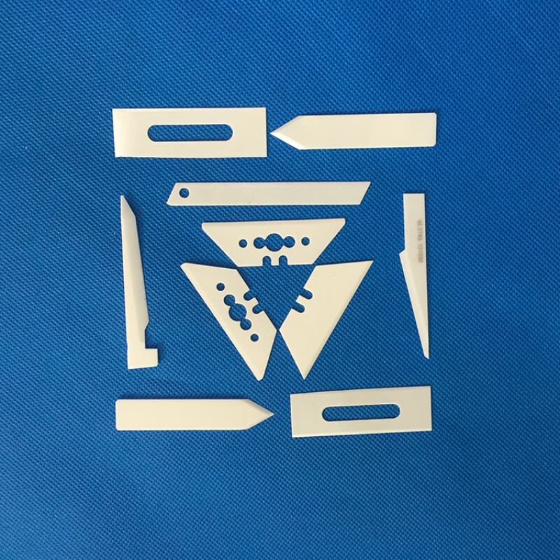
What Is Sapphire Ceramic?
Sapphire ceramic is a high-purity single-crystal alumina (Al₂O₃) with a hexagonal (rhombohedral) crystal structure. Its manufacturing involves crystal growth methods such as the Kyropoulos or Czochralski process, followed by precision slicing, lapping, and polishing to achieve the required orientation and surface finish. Common crystallographic orientations include C-plane (used for GaN epitaxy), R-plane (for silicon-on-sapphire applications), and A-plane.
Sapphire is classified as a technical ceramic but differs fundamentally from other alumina products due to its single-crystal structure. This eliminates grain boundary effects, resulting in superior mechanical strength, higher thermal conductivity, and lower dielectric loss compared to polycrystalline alternatives.
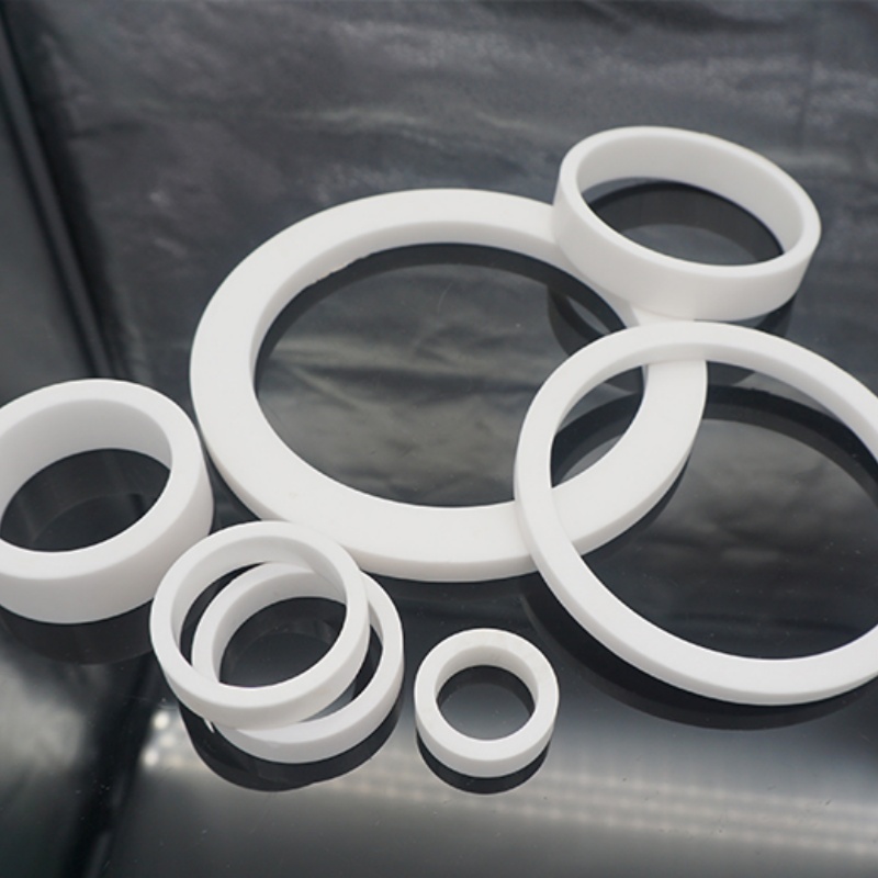
Key Properties of Sapphire Ceramic
Sapphire ceramic offers a combination of properties essential for semiconductor manufacturing environments:
Mechanical Properties
– Hardness: 9 on the Mohs scale, comparable to tungsten carbide
– Flexural strength: ≥ 500 MPa, enabling thin, robust component designs
– Compressive strength: up to 2 GPa, supporting high-load structural applications
– Modulus of elasticity: approximately 56 × 10⁶ psi, providing excellent rigidity
Thermal Properties
– Melting point: 2040°C, suitable for high-temperature processes
– Thermal conductivity: 42 W/m·K, facilitating efficient heat dissipation
– Coefficient of thermal expansion: 7.0–7.7 µm/m·°C, closely matching silicon, minimizing thermal stress at interfaces
– Maximum working temperature: up to 1900°C in inert atmospheres
Electrical Properties
– High electrical resistivity and low dielectric loss, ideal for high-frequency applications and plasma environments
– Excellent electrical insulation, preventing leakage in high-voltage equipment
Chemical and Plasma Resistance
– Inert to most acids, alkalis, and process chemicals used in semiconductor manufacturing
– Outstanding plasma resistance, minimizing particle generation in etching and CVD chambers
Optical Properties
– Transparency from UV (0.14 µm) to IR (6 µm), enabling use in chamber windows and optical inspection components
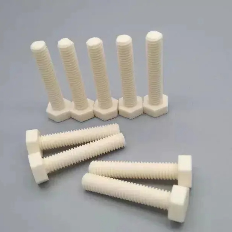
Advantages Compared with Other Ceramic Materials
When selecting materials for semiconductor equipment, understanding the comparative performance of sapphire is essential.
Sapphire vs. Polycrystalline Alumina (Al₂O₃)
Sapphire offers a lower dielectric loss tangent than alumina ceramics, critical for high-frequency and plasma applications. Its single-crystal structure eliminates porosity and grain boundaries, yielding superior mechanical strength and chemical resistance. The absence of grain boundaries also ensures minimal particle generation, a primary concern in cleanroom environments.
Sapphire vs. Fused Quartz / Glass
While fused silica offers lower cost and broad optical transmission, sapphire provides significantly higher hardness, thermal conductivity, and temperature resistance. Sapphire windows can withstand aggressive plasma cleaning and high-temperature bake-out cycles that would degrade glass components. For high-temperature viewports, sapphire’s mechanical strength enables thinner, more durable window designs.
Sapphire vs. Silicon Carbide (SiC)
Both materials exhibit excellent thermal and mechanical properties. However, sapphire provides electrical insulation (where SiC may be conductive or semi-insulating) and optical transparency, making it preferred for viewports and optical monitoring applications.
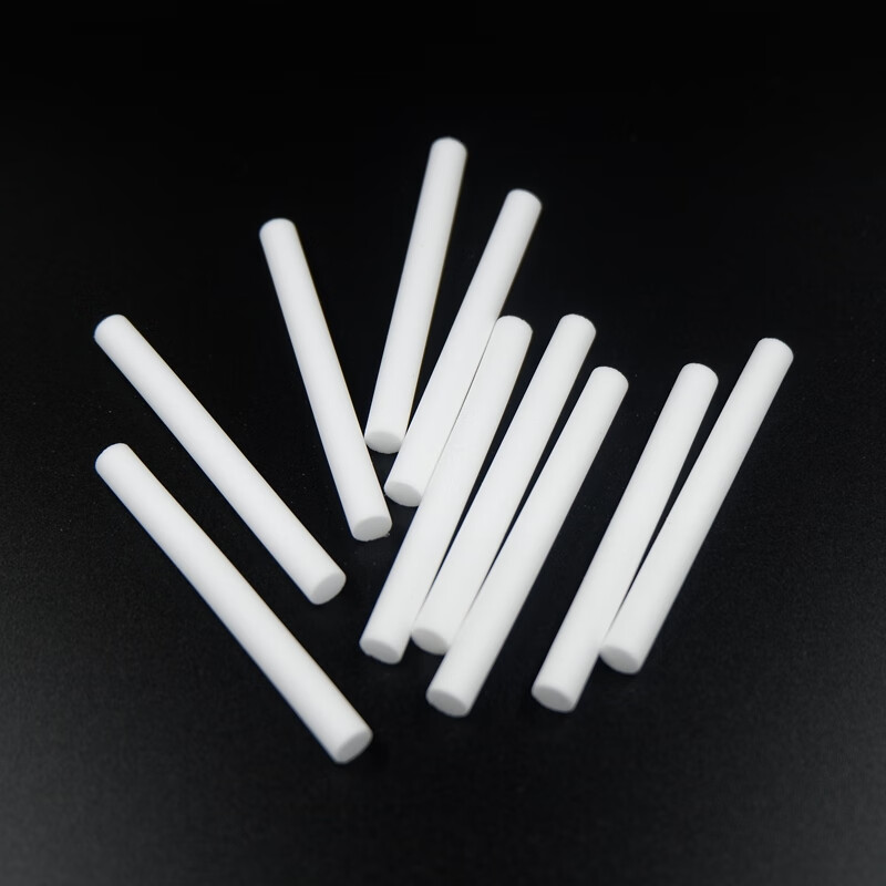
Custom Manufacturing Options
As a precision components specialist, a reliable manufacturer offers extensive customization capabilities for sapphire parts.
– Crystallographic Orientation: Selection of C, R, A, or M plane based on application (e.g., C-plane for epitaxial growth, R-plane for SOS devices)
– Geometry: Custom shapes including windows, rods, tubes, end effectors, boats, and flow cells
– Dimensions: Tolerances as tight as ±0.05 mm for dimensions under 1 mm, scaling to ±0.5 mm for larger components
– Surface Finishing: Lapping, polishing, grinding, and edge chamfering to meet specific roughness and flatness requirements
– Secondary Operations: Drilling, step processing, grooving, and metal fitting assembly
– Joining: Direct bonding of sapphire-to-sapphire or sapphire-to-alumina for complex fluidic and optical structures
Working with an OEM that provides custom parts ensures that components are optimized for specific tool designs, process conditions, and performance requirements.
How to Choose the Right Supplier
Selecting a supplier or factory for sapphire ceramic components requires evaluation beyond price. Consider the following criteria:
Material Quality and Purity
Specify purity requirements; semiconductor applications typically demand ≥ 99.99% purity to minimize contamination risk. Request material certifications and impurity analysis reports.
Technical Capability
Assess the manufacturer’s ability to produce required geometries, tolerances, and surface finishes. Inquire about in-house capabilities for crystal growth, shaping, and precision machining. A vertically integrated factory often provides better quality control and supply chain reliability.
Quality Systems
Look for ISO 9001 or IATF 16949 certification, with documented process controls, inspection protocols, and traceability. For semiconductor applications, particle control protocols and cleanroom manufacturing may be required.
Engineering Support
A competent supplier provides application engineering assistance, helping with material selection, design optimization, and tolerance specification. This is particularly valuable for OEM projects requiring close collaboration.
Track Record and References
Review case studies and customer references, particularly from semiconductor equipment manufacturers. Established manufacturers typically have long-term relationships with industry leaders.
Sapphire ceramic stands as a high-performance, precision-engineered material in semiconductor manufacturing. Its combination of mechanical strength, thermal stability, chemical inertness, and optical transparency—unmatched by most alternative ceramics—makes it the material of choice for critical components exposed to aggressive plasma, high temperatures, and corrosive chemistries.
When selecting sapphire components, specify material purity, crystallographic orientation, and dimensional tolerances appropriate for the application. Partnering with an experienced manufacturer that offers custom parts and technical support ensures optimal performance and reliability. As semiconductor fabrication processes continue to advance, sapphire’s unique property set ensures its ongoing relevance for next-generation equipment.
FAQ
What is the difference between sapphire and alumina ceramic?
Sapphire is a single-crystal form of Al₂O₃, while alumina ceramic is polycrystalline. Sapphire exhibits higher mechanical strength, lower dielectric loss, better transparency, and superior chemical resistance due to the absence of grain boundaries.
Why is sapphire used in semiconductor manufacturing equipment?
Sapphire offers an exceptional combination of plasma resistance, high-temperature stability, low particle generation, and optical transparency in UV-IR ranges. These properties are critical for etching/deposition chamber components, wafer handling tools, and optical viewports.
What tolerances can be achieved for custom sapphire parts?
Standard dimensional tolerances depend on nominal size: for dimensions under 1 mm, ±0.05 mm is achievable; for dimensions up to 4 mm, ±0.1 mm; and up to 25 mm, ±0.2 mm. Tighter tolerances may be possible for specific applications and geometries.
How do I specify sapphire components for a semiconductor application?
Key specifications include: crystallographic orientation (C, R, A, or M plane), purity level, dimensions and tolerances, surface finish (roughness and flatness), and any secondary features such as holes, steps, or bonding requirements. Discuss the specific process environment (plasma type, temperature, chemicals) with your supplier to optimize material and design choices.
What should I look for in a sapphire components supplier?
Evaluate the supplier’s material purity certifications, manufacturing capabilities (especially in-house machining and polishing), quality management systems, and engineering support. References from semiconductor industry clients and a demonstrated track record in similar applications are also valuable indicators.
 What Is Polyimide (PI)
What Is Polyphenylene Sulfide (PPS)
What Is Polyimide (PI)
What Is Polyphenylene Sulfide (PPS)
 What is PEEK-for Engineers and Buyers
 Application Scope of Zirconia Ceramic Structural Components