
Ceramic Vacuum Chucks
In high-end manufacturing sectors such as semiconductors, display panels, and photovoltaic cells, competition over product performance is no longer limited to chip size or process nodes alone, but has extended to every detail of the manufacturing process. Particularly as wafers and glass substrates continue to evolve toward being “thinner, larger, and more brittle,” securing workpieces both firmly and safely during processing and handling has become a critical process challenge that cannot be overlooked.
What Is Ceramic Vacuum Chuck?
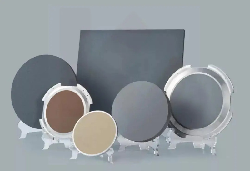
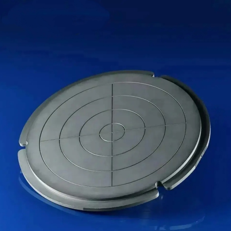
Ceramic vacuum chuck is an ultra-high-precision process fixture based on the principle of vacuum adhesion. It is primarily made of advanced ceramic materials such as aluminum oxide, aluminum nitride, or silicon carbide. Through precision-machined vacuum channels or porous structures on its suction surface, it connects to an external vacuum system to create a uniform negative pressure field.
In high-end manufacturing sectors such as semiconductors and display panels, the core value of ceramic vacuum chucks lies in the fact that they eliminate traditional mechanical clamping methods. By relying solely on uniformly distributed suction force, they can securely hold ultra-thin, ultra-brittle wafers or glass substrates under completely contactless conditions free from particle contamination. At the same time, thanks to its nanoscale surface flatness, extremely high rigidity, and excellent thermochemical stability, it provides a near-perfect positioning reference surface for workpieces in harsh process environments, thereby ensuring the precision and yield of critical processes such as lithography, inspection, and polishing.
Why Must It Be “Ceramic”?
In high-end manufacturing scenarios, a suction cup is not merely a simple “adhesion tool,” but a critical fixture that directly determines process stability and product yield. Among the many available materials, the widespread selection of ceramic materials precisely demonstrates how advanced ceramic materials systematically address industry pain points. From an engineering perspective, this can be summarized as the “Four Highs” requirements.
(1) High Flatness and High Rigidity
In semiconductor and display manufacturing processes, the silicon wafers and glass substrates being handled and processed are often as thin as a cicada’s wing, with thicknesses as low as several tens of micrometers. At this scale, even the slightest warping, vibration, or localized uneven stress can cause wafer breakage or warping, and may even directly affect the alignment accuracy of critical processes such as lithography.
Advanced ceramic materials (such as alumina and silicon carbide), through precision sintering and high-precision grinding and polishing processes, can achieve sub-micron or even nanoscale flatness. At the same time, their high elastic modulus endows the suction cups with extremely high structural rigidity, causing them to undergo virtually no deformation under vacuum suction, thereby providing an absolutely stable reference plane for the manufacturing process.
(2) High Purity and Chemical Inertness
Semiconductor manufacturing facilities have extremely stringent cleanliness requirements. Process fixtures must not only prevent particulate contamination but also avoid the leaching of metal ions and withstand repeated exposure to various cleaning chemicals.
As an inorganic non-metallic material, ceramic features a dense, smooth surface that is unlikely to generate particles; it is also non-magnetic, contains no migratable metal elements, and exhibits extremely high chemical stability. It maintains stable performance in environments containing strong acids, strong alkalis, or organic solvents, making it highly suitable for long-term use in high-cleanliness manufacturing processes.
(3) High Durability and Long-Term Stability
On automated production lines operating 24/7, ceramic suction cups must withstand tens of thousands of attachment and release cycles while enduring long-term temperature fluctuations and even high-temperature process environments. This places extremely high demands on the material’s wear resistance, fatigue resistance, and thermal stability.
Compared to metals or polymers, ceramics offer higher hardness and wear resistance, along with stable thermal expansion behavior, making them less prone to creep or performance degradation. Their service life is typically significantly longer than that of suction cups made from traditional materials, resulting in lower maintenance and replacement frequencies; from a total life-cycle cost perspective, they are actually more economical.
(4) Highly Integrated Functional Design
In more advanced semiconductor processes, the functionality of ceramic suction cups is no longer limited to vacuum adhesion. For example, in vacuum chambers used for dry etching, thin-film deposition (CVD/PVD), and similar applications, traditional vacuum ports may disrupt the chamber’s atmosphere and pressure distribution.
In such cases, “electrostatic chucks (ESCs)” serve as a critical solution. ESCs utilize the electrostatic force generated by a ceramic dielectric layer under an applied electric field to hold wafers. This not only prevents vacuum ports from disrupting the process environment but also allows for the integration of heaters and cooling channels within the chuck, enabling precise control of wafer temperature (from low temperatures to over 500°C). This makes ESCs an essential foundation for the successful implementation of advanced processes.
Typical Applications of Ceramic Suction Cups
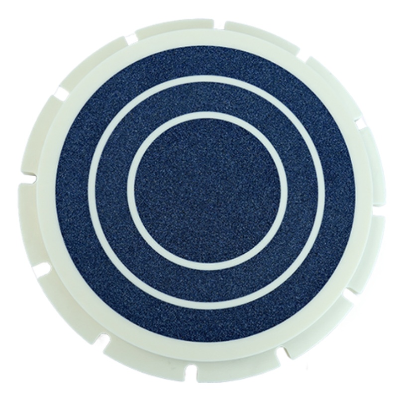
Ceramic suction cups are widely used in high-end manufacturing sectors such as semiconductors, display panels, photovoltaics, and precision optics.
In semiconductor processes, they serve as critical stages for lithography, etching, polishing, and inspection; in the display panel industry, they provide stable support and transport for large-size, ultra-thin glass substrates; and in photovoltaic cell production, they ensure the safe handling of thin, brittle silicon wafers during processes such as cutting and testing.
Their core value lies in providing a precision clamping solution—free from mechanical stress and particulate contamination—for ultra-thin, ultra-flat, and ultra-brittle workpieces, serving as the cornerstone for ensuring yield and efficiency in modern precision manufacturing. Although ceramic suction cups do not directly participate in “manufacturing,” they make manufacturing possible; though they do not appear in the final product, they profoundly influence product yield and consistency. As advanced manufacturing places ever-increasing demands on precision, cleanliness, and reliability, the importance of ceramic suction cups is being increasingly recognized across a growing number of industries.
 What Is Polyimide (PI)
What Is Polyphenylene Sulfide (PPS)
What Is Polyimide (PI)
What Is Polyphenylene Sulfide (PPS)
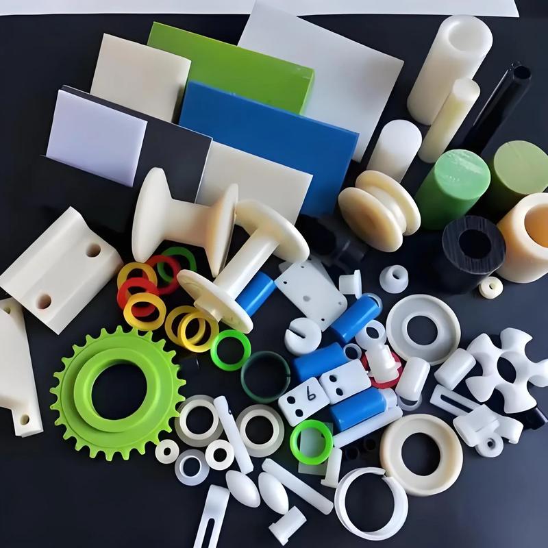 What is PEEK-for Engineers and Buyers
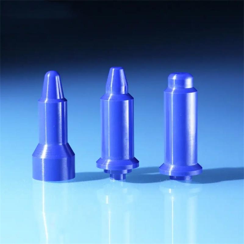 Application Scope of Zirconia Ceramic Structural Components