
Alumina Ceramic in Semiconductor Manufacturing Equipment
Alumina ceramic (aluminum oxide, Al₂O₃) has become a foundational material in semiconductor fabrication, serving as a critical enabler for advanced chip production. In semiconductor manufacturing environments—where plasma corrosion, high temperatures, and extreme cleanliness requirements converge—alumina ceramic components provide the stability and reliability that process engineers demand. From etching chambers to wafer handling systems, this advanced ceramic material plays an indispensable role in maintaining process integrity and yield.
The semiconductor industry’s shift toward larger wafers and smaller feature sizes has intensified the need for materials that can withstand increasingly aggressive conditions without contaminating the process environment. Alumina ceramic, with its proven combination of electrical insulation, thermal stability, and chemical resistance, has emerged as a preferred solution for equipment manufacturers and chipmakers alike .

What Is Alumina Ceramic for Semiconductor Applications
Alumina ceramic is a polycrystalline material composed primarily of alpha-phase aluminum oxide (α-Al₂O₃). For semiconductor applications, purity grades typically range from 95% to 99.9%, with higher-purity variants offering superior performance in demanding process environments . The material is manufactured through powder processing, forming, and high-temperature sintering—processes that require precise control to achieve the required density, grain structure, and mechanical properties.
What distinguishes semiconductor-grade alumina ceramics from conventional industrial grades is the stringent control of impurities and microstructure. Advanced manufacturing techniques, including cold isostatic pressing, gel casting, and precision machining, enable the production of components with complex geometries and tight dimensional tolerances .
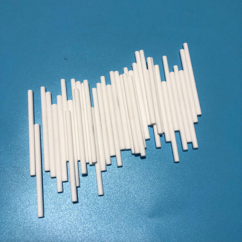
Key Properties of Alumina Ceramic for Semiconductor Equipment
Mechanical Properties
Alumina ceramic exhibits high flexural strength (350–500 MPa for 99.5%–99.9% purity grades) and excellent compressive strength exceeding 2800 MPa. These Mechanical Properties ensure component integrity under mechanical loads and thermal stresses encountered during wafer processing .
Electrical Insulation
With volume resistivity exceeding 10¹⁴ Ω·cm and dielectric strength of 15–18 kV/mm, alumina ceramic provides exceptional Electrical Insulation essential for RF plasma applications and electrostatic chucks. The material maintains stable dielectric properties across a wide frequency range .
Thermal Conductivity
Thermal Conductivity values of 20–33 W/(m·K) allow efficient heat dissipation from critical process zones. This property is particularly valuable in deposition and etching equipment where temperature uniformity affects process outcomes .
Wear Resistance
The high hardness (Vickers hardness >15 GPa) translates into exceptional Wear Resistance, enabling components to withstand particle abrasion from plasma etching and wafer handling without generating contaminants .
Corrosion Resistance
Alumina ceramic demonstrates strong Corrosion Resistance against halogen-based plasma gases (fluorine, chlorine compounds) used in etching and cleaning processes. The material’s chemical inertness prevents reaction with process byproducts, maintaining chamber cleanliness .
High Temperature Resistance
The material maintains structural integrity at temperatures up to 1500°C–1600°C, supporting High Temperature Resistance requirements in thermal processing steps such as oxidation and diffusion .
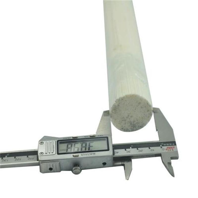
Typical Applications
Chamber Liners and Inner Walls
In etching and deposition equipment, chamber liners fabricated from high-purity alumina create a protective barrier between plasma and the metal chamber body. These components prevent metal contamination while maintaining electrical isolation. Field data indicate that alumina liners with ≥99.5% purity maintain dimensional deviation below 0.08 mm after 1800 process hours .
Gas Distribution Components
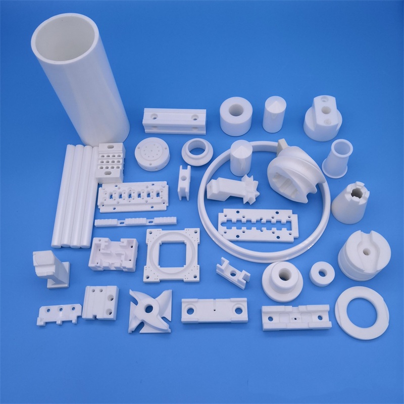
Nozzles, gas rings, and showerheads require precise internal geometries and excellent plasma resistance. Alumina ceramic’s machinability and Corrosion Resistance make it an ideal choice for these gas distribution parts .
Wafer Handling Components
Ceramic mechanical arms, end effectors, and wafer chucks must provide clean, particle-free wafer transport. Alumina’s hardness and Wear Resistance ensure long service life while maintaining the low particle generation required for Semiconductor cleanliness standards .
Insulating Components
Insulating rings, flanges, and spacers separate electrical potentials in RF-driven systems. The material’s stable Electrical Insulation properties prevent arcing and signal interference in critical equipment .
Process Equipment Accessories
Polishing plates, vacuum chucks, and structural supports in Chemical Mechanical Planarization (CMP) equipment benefit from alumina’s hardness and corrosion resistance, ensuring consistent performance in abrasive, chemically aggressive environments .

Advantages Compared With Other Ceramic Materials
Alumina ceramic occupies a unique position in the semiconductor materials spectrum. While Aluminum Nitride offers superior Thermal Conductivity for heat-intensive applications, and Silicon Carbide provides exceptional stiffness and thermal performance, alumina remains the preferred choice where cost-effectiveness, proven reliability, and stable Electrical Insulation are primary considerations .
In plasma environments, high-purity alumina surfaces exhibit erosion rates below 0.5 µm per 1000 process hours—outperforming many coated metal alternatives that show coating delamination after 400 hours . This performance advantage, combined with lower material cost and established manufacturing infrastructure, makes alumina the most widely used ceramic in semiconductor equipment, accounting for approximately 45% of the precision ceramic components market .
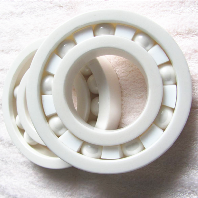
Custom Manufacturing Options
For semiconductor applications, Custom Parts fabrication requires specialized capabilities that distinguish leading Manufacturers from general ceramic suppliers.
Material Purity Selection
Alumina purity levels range from 95% to 99.9%, with semiconductor applications typically requiring ≥99.5% purity to minimize contamination risks. The choice of purity grade affects not only performance but also manufacturing feasibility and cost .
Forming Technologies
OEM suppliers employ multiple forming technologies to achieve the required geometries and properties:
– Dry pressing for simple shapes with good dimensional control
– Cold isostatic pressing (CIP) for uniform density in larger components
– Gel casting for complex near-net shapes
– Injection molding for high-volume, intricate designs
Precision Machining
Semiconductor components demand tight tolerances—often within ±0.05 mm—and surface finishes as fine as Ra 0.05 µm. Advanced machining capabilities, including CNC milling, grinding, and lapping, are essential for producing Precision Components that meet equipment manufacturer specifications .
Quality Assurance
Reputable Suppliers implement comprehensive quality control programs, including dimensional inspection, density measurement, surface finish analysis, and material purity verification. ISO 9000 certification and cleanroom manufacturing capabilities are indicators of established quality systems .
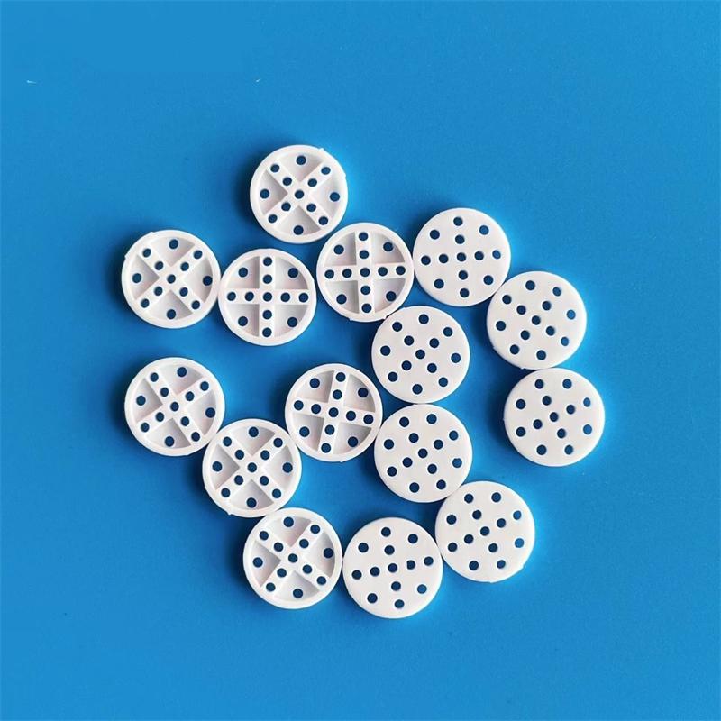
How To Choose The Right Supplier
Selecting an alumina ceramic Supplier, Manufacturer, or Factory for semiconductor applications requires careful evaluation of technical capabilities and quality systems.
Technical Capability Assessment
Evaluate the supplier’s experience with semiconductor applications, including their understanding of purity requirements, contamination control, and plasma resistance testing. Suppliers with proven track records in semiconductor equipment manufacturing—such as those supplying major OEMs like Applied Materials, Lam Research, and Tokyo Electron—demonstrate established quality systems .
Manufacturing Infrastructure
Assess the Factory’s processing equipment, including:
– High-temperature sintering furnaces with precise atmosphere control
– Precision grinding and machining equipment
– Cleanroom facilities for final processing and packaging
– In-process inspection and metrology tools
Customization Support
The ability to provide Custom Parts through collaborative design, prototyping, and production scale-up distinguishes capable Suppliers. Look for Manufacturers offering engineering support for material selection, tolerance optimization, and structural design .
Supply Chain Reliability
Evaluate the Supplier’s production capacity, lead times, and quality consistency. For critical Semiconductor applications, supply chain disruptions can have significant operational impacts. The global supply landscape is dominated by Japanese companies (Kyocera, NGK, Ferrotec) and US-based CoorsTek, with increasing participation from Chinese Manufacturers achieving comparable quality levels .
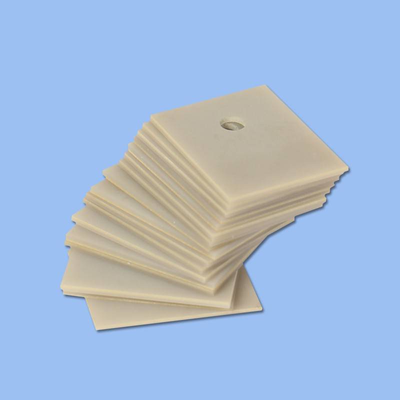
Alumina ceramic has established itself as the most widely used advanced ceramic in semiconductor manufacturing equipment, combining proven reliability, cost-effectiveness, and performance characteristics that align with industry demands. Its unique combination of Electrical Insulation, Corrosion Resistance, Mechanical Properties, and Thermal Conductivity supports critical functions in etching, deposition, and wafer handling equipment.
For procurement professionals and engineers evaluating material solutions, understanding the relationship between alumina purity, manufacturing processes, and component performance is essential for making informed decisions. As semiconductor processes continue to push toward 3 nm and beyond, the demand for high-purity, precision-engineered alumina components will grow—making the selection of qualified Suppliers a strategic priority .
Frequently Asked Questions
Why is alumina ceramic used in semiconductor manufacturing equipment?
Alumina ceramic is used in semiconductor equipment because it provides a unique combination of properties: excellent electrical insulation for RF applications, chemical resistance against aggressive plasma gases, mechanical strength for structural integrity, and low particle generation that protects wafer cleanliness. These properties make it essential for chamber liners, wafer handling components, and insulating parts .
What is the difference between 95%, 99%, and 99.5% alumina purity grades?
Higher purity grades offer improved corrosion resistance, better electrical insulation stability, and lower contamination potential. However, they are more expensive and difficult to manufacture. Semiconductor applications typically require ≥99.5% purity. The 95% grade is common for general Industrial Equipment applications, while semiconductor-grade components demand the highest purity levels to minimize metal ion contamination risks .
How do I select the right alumina grade for my semiconductor application?
Selection depends on the specific process conditions: plasma composition (fluorine-based vs. chlorine-based), operating temperature, required electrical properties, and contamination sensitivity. For aggressive plasma etching environments, 99.5% or higher purity is recommended. For less demanding applications, 95%–99% purity may be sufficient. Consulting with an experienced Supplier’s engineering team is recommended for optimal material selection .
What should I consider when ordering custom alumina ceramic parts?
Key considerations include: required dimensional tolerances (typically ±0.05 mm for precision components), surface finish requirements (Ra 0.05–0.6 µm), purity grade specification, and post-processing needs (lapping, polishing, or coating). Ensure your Supplier has the necessary forming and machining capabilities for your part geometry. Requesting samples and verifying quality control systems are essential steps .
Which companies are leading suppliers of alumina ceramic components for semiconductor equipment?
Leading global Manufacturers include Japanese companies (Kyocera, NGK, Ferrotec, Niterra), US-based CoorsTek, and European suppliers like CeramTec. Chinese Manufacturers, including Kema Technology and ADCERAX, have demonstrated increasing technical capability and supply chain reliability, with some establishing direct supply relationships with major semiconductor equipment OEMs .
How do alumina ceramic components contribute to semiconductor yield improvement?
Alumina components contribute to yield improvement primarily through contamination control and process stability. Low particle generation minimizes wafer defects, while dimensional stability ensures consistent process geometry over thousands of operating cycles. The material’s predictable wear behavior enables proactive maintenance scheduling, reducing unexpected downtime .
 What Is Polyimide (PI)
What Is Polyphenylene Sulfide (PPS)
What Is Polyimide (PI)
What Is Polyphenylene Sulfide (PPS)
 What is PEEK-for Engineers and Buyers
 Application Scope of Zirconia Ceramic Structural Components